A BROADBAND, SOLID STATE AMPLIFIER FOR
HF AND 6 METERS.
Pieter Ibelings, N4IP
Pieter@ibelings.com
I. INTRODUCTION
In 1986 Helge Granberg of Motorola published an article describing the design and construction of a MOSFET solid state kilowatt amplifierplifier using MOSFET's. Helge's work was followed by articles that appeared in QEX and QST by Joel F. Paladino, N6AMG. Since then, very little has been written in amateur radio publications concerning MOSFET’s in kilowatt applications. Most kilowatt amplifier designs published, use vacuum tubes. These amplifiers tend to be bulky and heavy. In this article, I hope to renew interest in high power solid state RF devices. My primary objectives are to revisit the designs, investigate the use of newer devices, and offer a creative implementation of these devices in an amateur radio amplifier. Please keep in mind, this amplifier design is a work in progress.
II. TUBES VS. BIPOLAR VS. MOSFET'S
Previously, I contemplated building an amplifier using vacuum tubes. My requirement was for an amplifier in the 1000 Watt class for HF and six meters. In addition, I needed a power device that would handle this requirement. The device that came to mind was a Eimac 8877. I researched a design that would cover HF through Six meters. Every design was either for HF or Six meters, but not for both. In addition, they involved tube technology which I had not worked with in the past. The designs also looked a bit more mechanically complex than I had expected. My idea was to aim for a design that was both portable and straight forward to implement.
After weighing the pros and cons, it looked like a solid state design was the only viable option left. But which devices should I use? Bipolars or MOSFET's? After a lot of reading, it seemed like MOSFET's would be the device of choice. I decided to build one of the amplifiers designed by Helge Grandberg of Motorola.
I had remembered reading of a design in QST, so I decided to go through all my piles of magazines. I finally found the article in the September 1992 issue. By looking at the schematic, everything looked very straight forward and simple. The device used was an MRF154 MOSFET in a push-pull configuration.
III. MOSFET's
MOSFET's (Metal-Oxide-Semiconductor Field Effect Transistors) offer a lot of advantages over bipolar devices. The main advantage is higher input impedances. This allows better matching networks to be incorporated, creating an amplifier with a broader bandwidth. In addition, they also offer superior stability than bipolars. Who wants an oscillating kilowatt amplifier? MOSFET’s are also more robust than bipolars. MOSFET’s tend to be harder to overdissipate except when an overvoltage condition exists. MOSFET’s are also capable of more power per device. This makes kilowatt amplifiers easier to design without the need of complicated and lossy combiners. One disadvantage of Bipolars is that they suffer from thermal runaway. This means that current gain increases with temperature. In turn, this causes the device to draw more current as it gets hotter, thus causing an even greater temperature increase. MOSFET's are the opposite. Their gains decrease as temperature increases, causing the device to want to turn off. One drawback of FET's is that their low order distortions are a little worse than those of bipolars. They do however, offer acceptable performance for ham radio use.
The MOSFET is a device in which current flow is controlled by an applied electric field. There are two modes of operation. These are as follows:
Enhancement Mode. When the gate voltage is zero, these type of devices do not conduct current across the channel. The drain current increases with applied gate voltage. The name enhancement comes from fact that the channel is enhanced by an increased gate voltage; increasing drain current. These devices are analogous to a closed water faucet. Applying a voltage to the gate opens the faucet, increasing water flow. Water flow is equivalent to drain current in this example.
Depletion Mode. These devices conduct with zero applied gate voltage. The name depletion comes from the fact that the device channel needs to be depleted in order to reduce the drain current. In "N"-Channel devices, a negative voltage is applied to the gate. Similar to the above, these devices are analogous to an open water faucet. Applying a voltage to the gate closes the faucet, decreasing water flow. Most FET's used in pre-amplifier circuits are depletion devices while those used in very high power amplifiers are mostly of the enhancement types.
IV. HF to Six, 1200W Amplifier
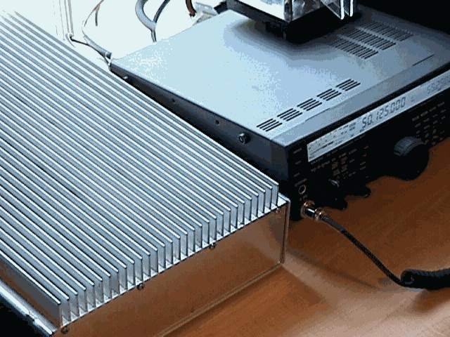
My device of choice was, the MRF157 instead of the MRF154. This device seemed to be identical to the MRF154, with the addition of a little higher gain. After securing the transistors, I had to find a big enough heatsink that could dissipate all this heat. Each MRF157 is capable of dissipating a minimum of 600 Watts. A visit to my employer's dumpster paid off. With the help of a friend I managed to pull a 16 x 10 inch heatsink with 1 inch fins from under piles of aluminum rubble. The heatsink (figure 1) was in great shape. It only required a milling machine to straighten the edges and improve the surface accuracy. Due to the high power dissipation of this amplifier, it is very important that all heatsinking surfaces are within thousands of an inch. If the heat from these devices is not properly dissipated, the devices will fail.
A couple of days later, a friend offered to smoothen the heatsink for me. Next, I decided to get an aluminum box for the amplifier (3 inches high) which provided enough room to fit all the support electronics. The custom aluminum enclosure was ordered from Byers Chassis Kits. I then gathered all the necessary components to start building the RF module. Most parts for the RF module including the copper heat spreader are available from Communications Concepts. A copper heat spreader is required to dissipate the level of heat generated. Copper offers much lower thermal resistance than aluminum and satisfies the dissipation requirements.
Figure 1. Aluminum box and heatsink. (The radio to the right is an FT-847).
It took approximately two hours to build the two halves of the circuit board. I paid very close attention to the location of the bypass capacitors. It is very important that all the parts experiencing high RF currents are well soldered. I had decided that I would initially spend some time ensuring that the copper heat spreader to aluminum heatsink interface was perfectly matched. The aluminum heat sink was milled to within a couple of thousandths of an inch. I purchased an orbital sander to lightly sand the two sides. I used the lightest sand paper available. Due to a maintenance problem with the milling machine, I attempted to use the sander to complete the interface. Getting both sides to mate perfectly ended up being a very painstaking process. I sanded the copper spreader in a circular motion in order to get it as flat as possible. Then, I spread a very thin layer of heatsink compound uniformly on the copper plate. Using eight predrilled and tapped holes, both surfaces were mated tightly. Next, both surfaces were separated and examined to determine the heatsink compound distribution. I cleaned the compound off and sanded one of the two sides to increase contact in the bad areas. This process was repeated over twenty times and took over 12 hours, but I finally had an interface that had no air gaps. Don’t try this at home, use a milling machine. I ended up using 16 screws equally spaced to improve the contact area. It turned out that the copper was more flexible than I had imagined. Going from 8 to 16 screws greatly increased the contact area.
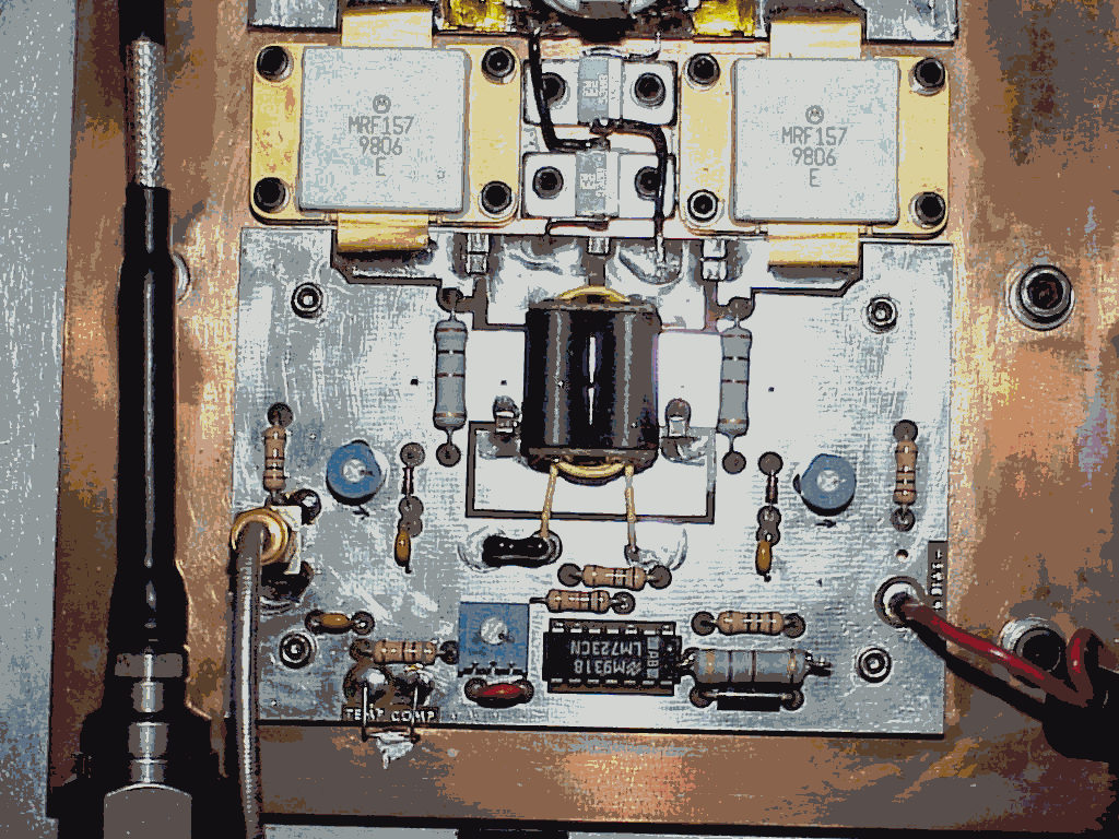
Figure 2 - Input Circuit Board Mounted To Copper Heat Spreader.
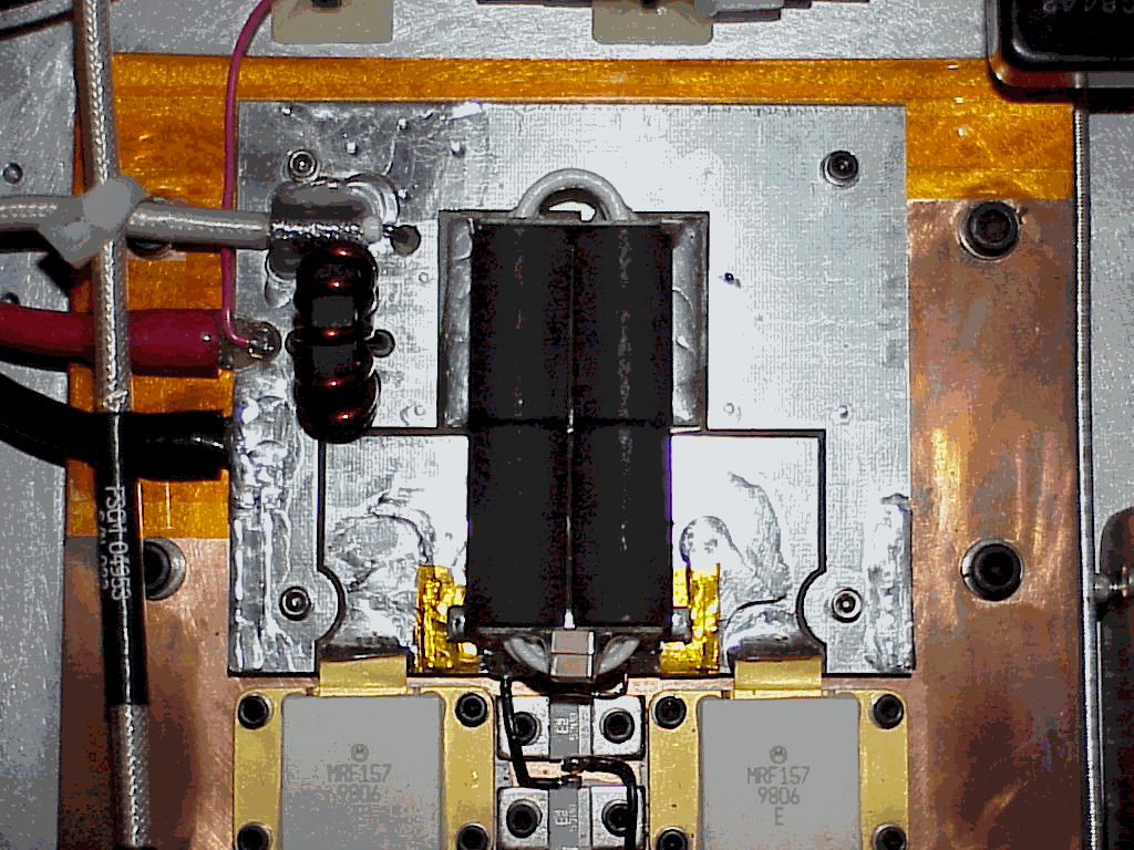
Figure 3 - Output Circuit Board Mounted To Copper Heat Spreader. Output Transformer Is Visible In The Center Of The Photo.
After completing both halves of the circuit board, I powered both sides independently without the FET's, to verify it's construction. I set both gate voltages to zero using the potentiometers. This would ensure that the FET's would not draw any current when powered for the first time. On the output section I verified that nothing was shorted by applying 50 volts to the board. This was the easy way of getting rid of shorts. Due to the 50 Amp capability of the supply any shorts would have vaporized in an instant. If you are opposed to this sort of trial by fire, use an ohm meter. I then proceeded to mount both boards to the copper heat spreader. I used 1/8 inch spacers for the board. It took a while to ensure that everything was spaced right. I marked the location of the holes and proceeded with the drilling. I used a drill press to insure that the holes were at right angles to the plate. The tapping process turned out to be very slow. It was real easy to break a tap in copper. At one point, I broke a tap and it took me an hour to remove the piece without ruining the copper plate. Before bolting both boards, I lightly sanded the area under the devices to ensure that the surface was flat. I then proceeded with the mounting of the boards. After the boards were mounted, I re-verified that nothing had shorted and then proceeded to install the FET's.
I was now ready to power up the RF module. Any mistake could be very costly. I don't remember how many times and from how many angles I checked the boards. I finally had enough courage to apply power to the board. I connected a coax cable to the output and terminated it in a 50 ohm load. It's important to load the amplifier at RF frequencies just in case of oscillations. I powered the amplifier with 48 volts and heard a small pop. I was not sure what it was, but I ended up taking everything apart and rechecking my work. It turned out to be a vibration in the transformer when power was first applied. I verified that the devices were not pulling any current and proceeded to set the idle current for both devices. I slowly increased the gate voltage of FET #1 until the current increased by 800mA. I then increased the current of FET#2 until the total current was another 800mA higher. This was all the biasing that had to be done. The amplifier was now ready for RF testing.
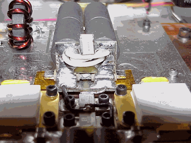
Figure 4 – View of output transformer soldered above silver mica capacitors. The two big chip capacitors on the top are used to cancel some of the stray inductance at 50 MHz. The two flanged resistors on the bottom are part of the feedback network.
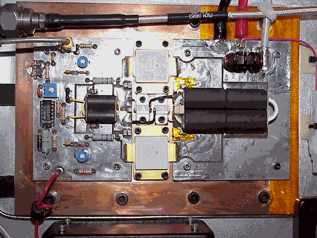
Figure 5 - Completed RF Module On Copper Heat Spreader. The Two Round Potentiometers Set The Idle Currents Of The FET's Independently.
Initial tests were run using a 44V linear supply (refer to table 1). I slowly verified the output at the different ham bands using a dummy antenna and calculated the efficiencies. Poor efficiency is an indication that something is wrong. The efficiency ranged from 35% at 400 Watts to 60% at 700 Watts (15 MHz). Some of the results are listed below:
Table 1. Power out using 44 Volts Supply
Frequency Output Power Input Power Current
|
50 |
610 |
10 |
30 |
|
14 |
600 |
10 |
28 |
|
10 |
740 |
10 |
28 |
|
5 |
790 |
25 |
37 |
|
50 |
790 |
25 |
37 |
The circuit used in this amplifier is optimized around 800 watts. It is not common for the efficiency to drop below 40% when using this amplifier at much lower power. At first I, was a little disappointed with the performance. I was expecting a lot more power. Further investigation showed that I had one main problem. My power supply was not capable of supplying the 50 or more volts required for this amplifier. I decided to modify and beef up the supply. The final voltage was a regulated 51 volts. Now the power supply was capable of 50 amps. I re-ran the tests at the new voltage and the result was over 1000 watts on all of the HF bands. The power and efficiency would drop as you went up towards 50 MHz. I re-read the different articles and concluded that I had two other problems. The output transformer I had used was a mix 61. This higher permeability material was intended for HF. A lower permeability material would saturate at higher power levels and extend my frequency upwards. I rewound the output transformer using a mix 67 material. Communication Concepts Inc. does not offer this transformer prewound, but they do offer the mix 67 cores.
The new transformer seemed to work a lot better. It appeared to have moved my efficiencies up higher in frequency. I still noticed a decrease in power at the high frequencies. It turned out that the stray inductances of the output transformer were reducing my power around 50 MHz. I added two 100pF ATC capacitors in parallel. The power suddenly jumped past 1000 Watts at six meters. Performance on the HF bands was very good in the 1300+ Watt range.
Table 2. Power out using 51 Volts Supply
Frequency Output Power Input Power Current
|
50 |
1090 |
30 |
42 |
|
28 |
1000 |
25 |
37 |
|
14 |
1240 |
20 |
43 |
VI. CONTROL AND PROTECTION CIRCUITRY
After spending all this time and money, I had to protect my investment. I had to watch out for the killers:
It seemed like the addition of a microprocessor to the amplifier would provide all the required protection. I built a small computer board using a Basic Stamp II. I added an 8 channel, 12 bit A/D converter. This chip, a MAX186, would allow me to read the status of the amplifier. I used two channels for the 24 and 50 volt supplies, two channels for forward and reflected voltages, two channels for temperature and the last two channels for bias conditions.
The temperature monitoring uses an AD590 temperature sensor. This IC makes it real easy to sense temperature. The IC is a temperature controlled current source. The chip sources 1 micro Amp per degree Kelvin. If the current is passed through a 1000 ohm precision resistor, the voltage across this resistor equals the temperature in degrees Kelvin divided by 1000. I am in the process of installing a pair of these devices, one next to each transistor.
The relay sequencing is performed by a hex inverter chip using capacitors and resistors to delay one relay from the other. When the PTT is applied, the output relay and the amplifier bias is energized first, then the input relay turns on allowing the RF drive to reach the input of the amplifier. This ensures that the amplifier is never hot switched. The timing between relays is currently set to 15 milliseconds.
I decided that It would be a lot more fail safe to have an independent sequencer. This way, if the computer chip malfunctioned or crashed, the sequencer would still take care of powering down the amplifier with no hot switching of the relays.
The SWR protection and power metering part of the amplifier uses a pair of ADC channels to sense the forward and reflected voltages using an SWR bridge. The program then converts the voltage to power and calculates the SWR from these two values. I initially had problems with the amplifier tripping out due to the dynamic nature of SSB. I decided to build a peak detector circuit so that the display would function properly. It turned out that I could not find a place to put the board , so I had to resort to another idea. I created a loop inside the firmware that checks the forward and reflected voltages 24 times in less than a second. It then picks out the highest of the measurements and those values are the ones displayed. This software peak detector works very well. When the SWR reaches 1.7 or the reflected power exceeds 100 Watts, the chip removes power from the sequencer and the amplifier unkeys.
The temperature protection circuitry uses two channels of the ADC. Each channel is connected to an Analog Devices AD590 chip. When the temperature reaches 40 degrees C, the chip energizes the fan relay and the unit starts to cool down. If for any reason the temperature exceeds 60 degrees C, the power to the sequencer is removed. Whenever the amplifier is tripped due to SWR or temperature, the firmware enters an endless loop that requires the power to be cycled.
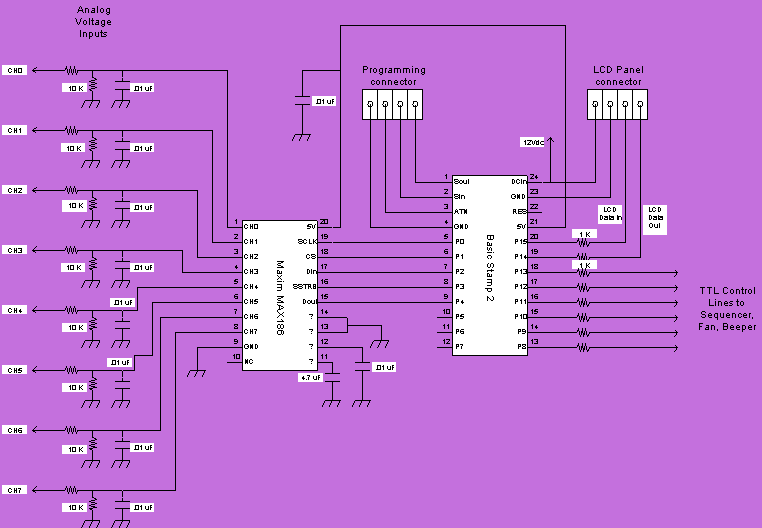
Figure 6 – Partial schematic of Basic Stamp II and ADC used to prevent damage to the amplifier. The analog inputs on the left are used to sense the voltages, temperature, and forward and reflected powers. The outputs on the right, turn the fans and sequencer on when needed. The outputs are TTL and require an open collector transistor to drive the relays.
Analog Inputs: Digital Inputs: Digital Outputs:
CH0 = Forward Voltage PTT In (P9) Input Relay (P12)
CH1 = Reflected Voltage Output Relay (P13)
CH2 = 50 Volt Supply Fan Relay (P10)
CH3 = 24 Volt Supply Bias On (P11)
CH4 = Bias 1 Beeper (P8)
CH5 = Bias 2
CH6 = Temp 1
CH7 = Temp 2
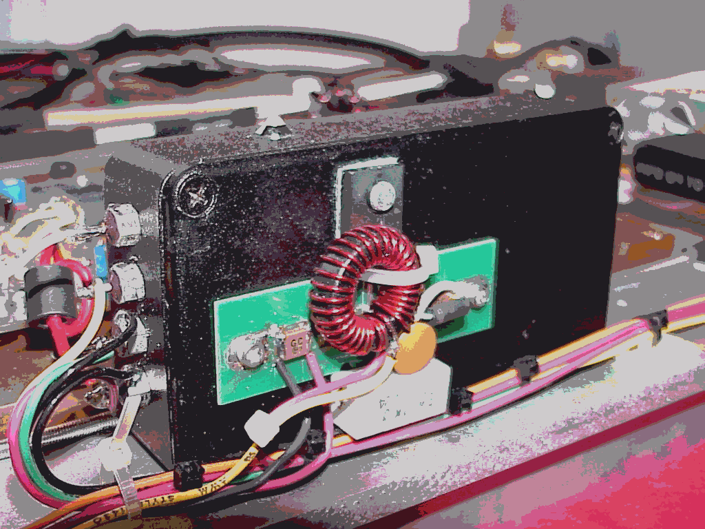
Figure 7 – Details of the 24 volt, high current regulator using a 2N3055. The 24 volts power the 12 volt regulator, fan and sequencer.

Figure 8 – Details of the relay sequencer using a hex inverter (HEF4069). The relay timing can be adjusted with the variable resistors.
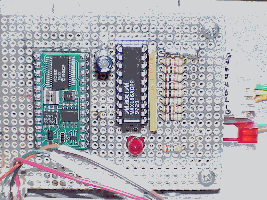
Figure 9 – Close-up of the Basic Stamp II and ADC.
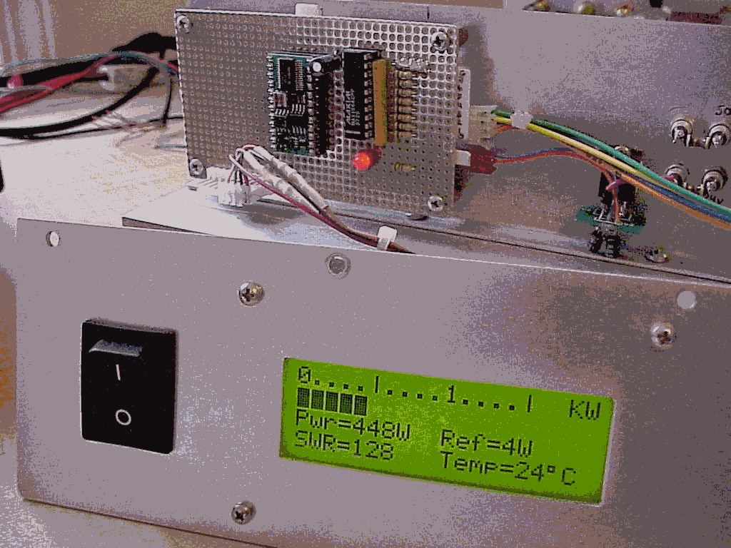
Figure 10 – Partially completed front panel showing the LCD by Orbital Matrix. The screen shown is during transmit. The bargraph shows the power output. The SWR is also calculated from the forward and reflected powers.
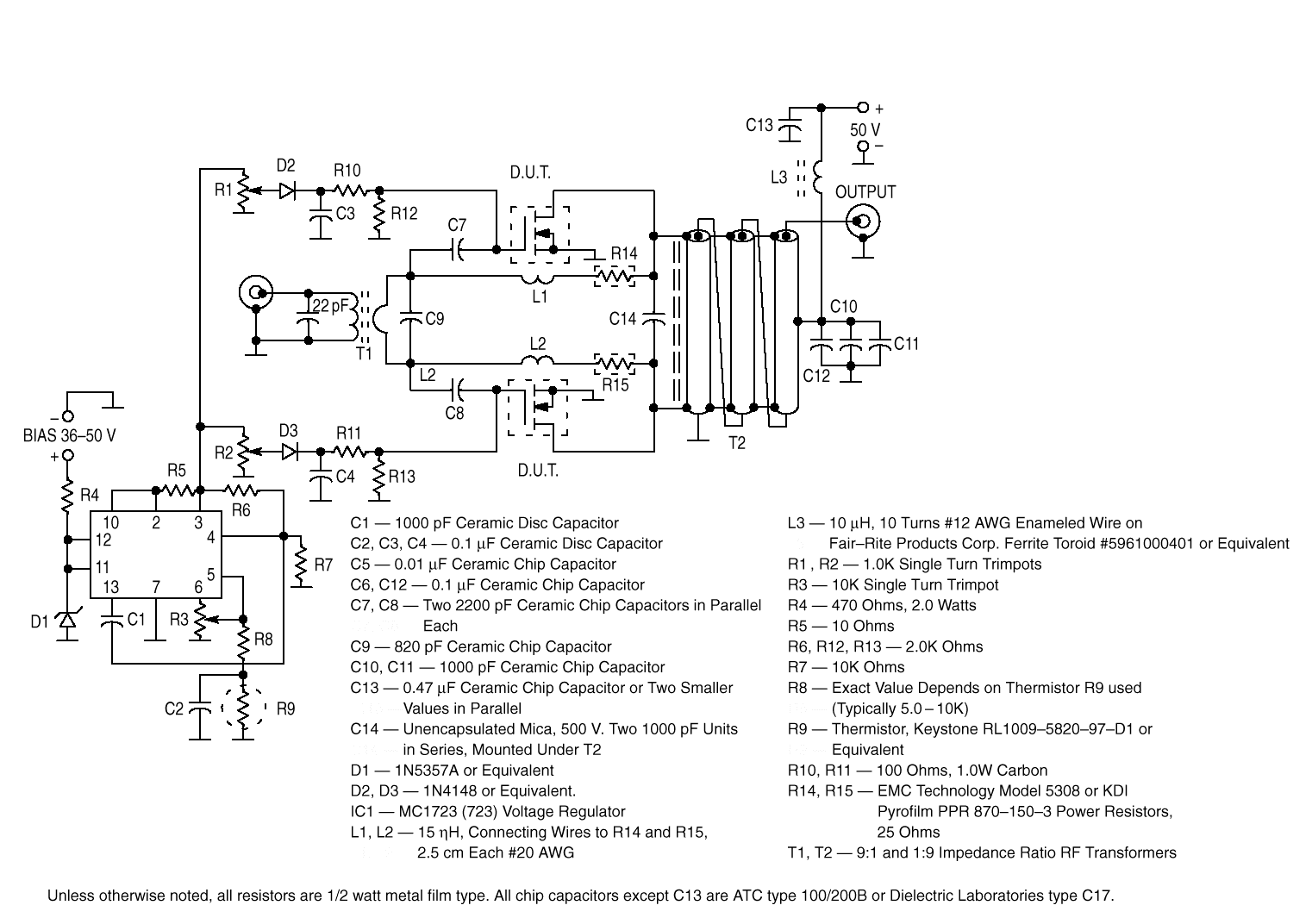
Figure 11 – RF Module schematic of the push-pull 2xMRF157 amplifier (from Motorola RF Device Databook DL110 Rev 7).
VII. CURRENT AMPLIFIER STATUS
Presently, this amplifier is still undergoing development. I am planning on incorporating a low pass filter bank to reduce second and third order harmonics. In addition, I am testing the amplifier at different bias conditions to determine which yields the best IMD performance. These results will be posted on my web site: www.ibelings.com/n4ip/mrf157.html. If you have any feedback please contact me via email at: pieter@ibelings.com.
VIII. SOURCE OF PARTS
CCI
http://www.communication-concepts.com/
CCI offers a complete line of parts kits for the Motorola designs. They also offer the copper heat spreader used in this amplifier.
Motorola -
http://www.mot.com
Motorola recently introduced a device that covers VHF and UHF and is capable of 300W. This device is the MRF275G.
Analog Devices-
http://www.analog.com
Analog Devices makes the temperature sensor used in this amplifier. This sensor can be purchased in small quantities from Newark Electronics.
Newark Electronics-
http://www.newark.com
Linux Central-
http://www.linuxcentral.com/products/modm/
Linux Central offers the complete line of Orbital Matrix LCD panels with serial data interfaces.
Byers Chassis Kits-
(717) 292-4901 6:00pm to 9:30pm EST
Chassis kits and custom enclosures.
Firmware for the Basic Stamp II-
http://www.ibelings.com/n4ip/mrf157.html
Firmware for this project is still under development. It will be available on the web page above as soon as it’s completed.
IX. NEWER DEVICES
Advanced Power Technology -
http://www.advancedpower.com
Advanced Power Technology has recently released low cost, plastic package devices suitable for HF and six meters. The ARF44X series of devices offer a cheaper alternative to the MRF157 devices used in this project. Refer to the following web sites for further information:
1000 Watt , 28 MHz amplifier at:
http://www.advancedpower.com/TechSupp/App_Notes/APT9701/
Description.html
250 Watt 6 meter amplifier at:
http://www.advancedpower.com/TechSupp/App_Notes/APT9702/
Description.html
500 Watt HF at:
www.picks.force9.co.uk/throb.htm
The amplifier described here uses regular switching FET’s like the IXFH58N20.
X. ACKNOWLEDGEMENTS
I wish to thank all the people who have helped me with the various aspects of the design. I specially thank Rafael Celedon, VE2HKI for all the hours spent over the phone. I also wish to thank Herm Kruse, W4GVO for all his help solving the RF and power supply issues. I could not have done this without the assistance of Brian Green, who procured the matched pair of transistors used in the amplifier. He was also involved in digging the heatsink used for this amplifier, out of our employer's dumpster. Last, but not least, I wish to thank Bob Simmers from Motorola for supplying me with parts and databooks for this project.
XI. REFERENCES